What is a mid-power CSP LED
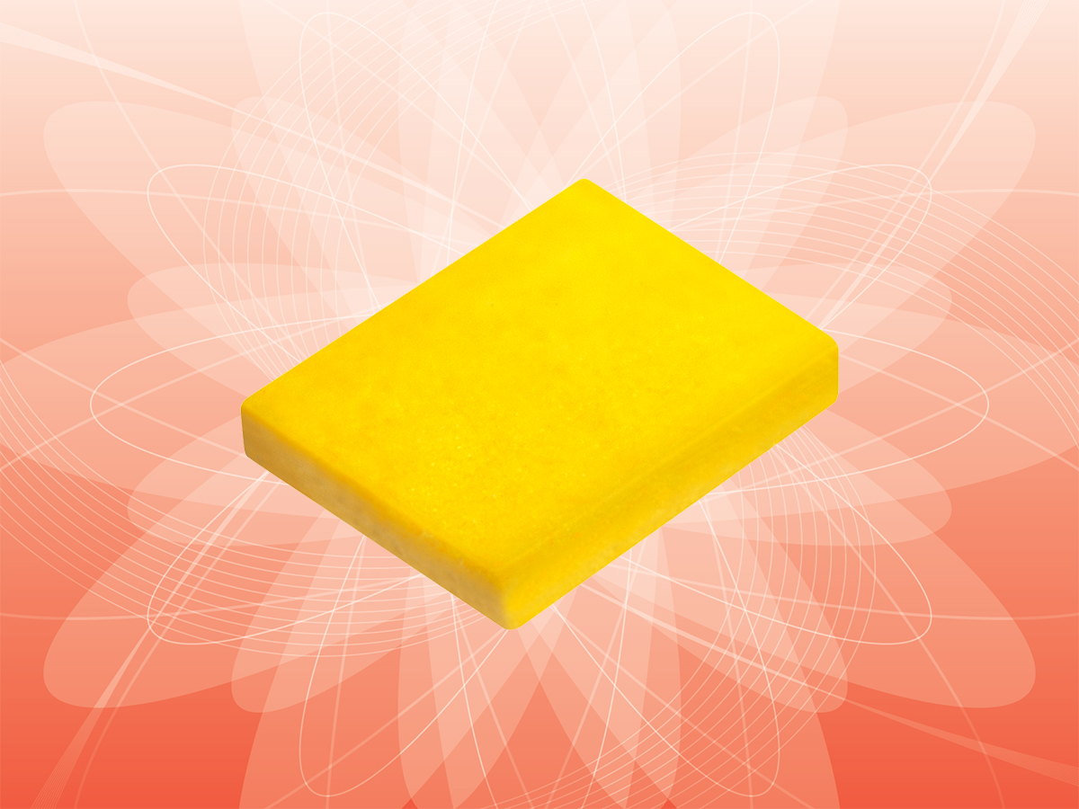
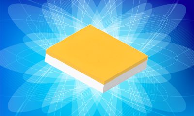
A mid-power CSP LED is a flat no-lead semiconductor emitter package that is constructed without using a lead frame and has both p-type and n-type electrical contacts on the bottom of the LED die. This type of LED package is designed as a lower-cost but higher-performance alternative to traditional plastic leaded chip carrier (PLCC) LEDs that operate at a low wattage (1 W max.). CSP LEDs are built around a flip-chip architecture which affords the lighting industry the opportunity to reduce both manufacturing and material costs while advancing the performance and reliability of the products to a new level. Chip-scale packages are invented with a philosophy to strip out as many of the superfluous package elements as possible. Along with the cost benefit are minimized thermal resistance, minimized length of the thermal path, maximized effective surface area for current and heat spreading, and a smaller footprint that enables unprecedented design freedom in optical control and new lighting form factors.
Light emission
The design of an LED package is a multidimensional engineering work that must address operational complexities presented by the technology. In optoelectronics, a light-emitting diode is a p-n junction that can convert electric power to light due to injection electroluminescence produced from active layers of semiconductor material sandwiched between oppositely doped semiconductor layers. When a forward bias is applied across the doped layers, negatively charged electrons in the n-type semiconductor and positively charged holes in the p-type semiconductor are injected into the active layer. Recombinations between charge carriers result in energy transitions in the excited electrons. Electrons drop down in energy from the conduction band to the valence band and release excess energy in the form of photons, which are the carriers of electromagnetic radiation. The difference in energy between the conduction band and valence band determines the wavelength of emitted photons. LEDs take advantage of the large energy band gap in direct band semiconductors, which allows photons to be emitted at wavelengths in the visible portion of the spectrum.
LED packaging
An LED p-n junction is a bare semiconductor die that serves as a light-emitting stack for electroluminescence to occur. Electromagnetic radiation produced by the device has a narrow wavelength distribution that is spectrally deficient for most visible lighting applications. The block of semiconductor materials is just simply a light-emitting element. It cannot be connected directly to an external circuit and mounted in any lighting system. The semiconductor die relies on a packaging structure to play its role. LED packaging is intended to provide mechanical, electrical and thermal interfaces to the semiconductor die. Mid-power LED packages are assemblies designed to be reflow soldered onto a printed circuit board (PCB) by making use of a standard surface mount technology (SMT) process. The package into which the LED die is assembled should provide interconnectivity that allows the LED junction to be connected to the load side of an LED driver, provides mechanical stability, and makes it possible for the heat generated at the LED junction to be conducted away in order to maintain expected light output, color points and service life. A wavelength converter is typically incorporated into the package to provide spectral modification. The LED die is encapsulated in order to avoid extrinsic failures due to exposure to humidity and environmental contaminants.
The downside of PLCC-based package architecture
The packaging of mid-power LED dies had been based around the PLCC architecture before the CSP platform was introduced. A PLCC-based mid-power package has a lead frame that mechanically supports the LED die and creates one of the two electrical contacts. The lead frame also serves as thermal conductor for junction-to-board heat transfer. In most cases, the lead frame is silver-plated to improve light reflectivity. It is embedded in a reflective polymer cavity and filled with a phosphor containing encapsulant. The second electrical contact is created by wire bonding. Electrical leads typically extend out from the package sides. While the packages have a competitive edge with regards to costs and efficacy, they don’t really deliver the value people expected from LED lighting. The plastic resin used to mold the reflective cavity is usually PPA or PCT. These polymeric materials have a poor stability when exposed to high operating temperatures and high energy photons. Over time these package materials can decompose, discolor, crack, or delaminate, ending up with a shortened service life due to intolerable lumen depreciation and chromaticity shift. The use of the polymer housing also significantly increases thermal resistance and consequently compromises heat transfer efficiency. Leadframe corrosion can occur when the silver plating is exposed to an atmosphere containing corrosive sulfur compounds. Under high electrical stresses and extreme thermal shocks, the bond wire can fuse or break and cause an open circuit.
Package design
Mid-power CSP LED packages are bare-bones LED die assemblies that use minimal packaging materials to achieve a maximal level of improvement in dependability and significantly scale down the size of an LED package. The term “chip scale package” refers to a packaged product with a footprint no more than 20% larger than the LED chip (die) itself. In the absence of a submount, a CSP LED bridges the semiconductor die to its system interface with higher reliability and higher performance interconnects. With the thermal resistance reduced to a minimum, a higher thermal load can be handled by the semiconductor package. Accompanying the removal of polymer housing and lead frame are improved lumen maintenance and color stability. CSP LEDs are wire-free packages. Bonding wire breakages are among the most common failures in LEDs and comprise a major concern because they are catastrophic. The breakage can be caused by high peak transient currents, repetitive and high-magnitude thermal cycles, voiding in the bonds, and long-term exposure to a high humidity environment. CSP technology provides a foolproof solution by eliminating wire bonding. Since the power density of the LEDs are no longer limited by wire bonding, CSP LEDs can be driven at a higher current density than previously possible with wire-bonded LEDs.
Die fabrication
At the heart of the CSP technology is the concept of integrating the light-emitting stack itself into the package design. An LED die is constructed using a single-crystal semiconducting material modified in two separate regions to create the p- and n-type semiconductor layers with differing electrical properties. Acceptor impurity atoms are incorporated into one part of the host crystal to produce an epitaxial p-region in which the majority carriers are holes. Donor impurity atoms in the other part the host crystal produce the epitaxial n-region in which the majority carriers are electrons. A lower band gap material is sandwiched between the p- and n-layers to form the active region where the charge carriers recombine to produce light. Gallium nitride (GaN) is the material of choice for the host crystal. It is a direct and wide bandgap material with excellent thermal and chemical stability. The GaN epitaxy is based a double heterojunction (DHJ) structure. The light-emitting stack is comprised of an active layer of indium gallium nitride (InGaN) which is interposed between the p-GaN layer and the n-GaN layer to create a quantum well (QW). Each epitaxial layer in the double heterojunction must be deposited with a high degree of control over thickness, composition, and the interfacial delineation. The energy band gap of the quantum well is controlled by manipulating the indium content in the InGaN alloy and its layer thickness.
Substrate technology
GaN epitaxy is performed a carrier wafer, or commonly known as a substrate. The substrate technology drives the fundamental performance, efficiency and costs of InGaN LEDs. Sapphire, by far, is the substrate of choice for heteroepitaxial growth of GaN for all types of epitaxy-based LEDs. Heteroepitaxy refers to growth of a semiconductor crystalline structure on foreign substrates such as sapphire, silicon carbide (SiC), and silicon (Si). Compared with the GaN-on-SiC and GaN-on-Si counterparts, the GaN-on-sapphire system creates the best balance among all variants. It enables scalable and cost-effective production of DHJ devices on an industrial scale. The quality of GaN epitaxial growth on sapphire substrates supports a relatively high quantum efficiency. The downside of this substrate technology is the large lattice mismatch to GaN, which can result in a range of issues. Lattice mismatch of 16% between GaN and sapphire leads to formation of crystalline defects knowns as threading dislocations in a marked quantity. The high dislocation density results in an increased rate of non-radiative Auger recombination in the active region and consequently an efficiency droop when the LEDs are operated at high temperatures. The crystalline defects can alter and degrade the electrical properties of the semiconductor layers, which can trigger failure-mechanisms such as electromigration, local overheating and thermal runaway under the combined force of high operating temperature and high power density. GaN-on-Si is a lower-cost alternative, but the lattice mismatch (17%) and CTE (33%) between GaN and Si are even bigger problems. Considerably higher quality GaN epitaxy can be achieved using SiC substrates. However, as with the homoepitaxially grown GaN-on-GaN devices, GaN-on-SiC LEDs are rarely employed in mid-power applications due to cost considerations.
Flip-chip packaging
Mid-power CSP LEDs are the latest evolution of flip-chip LEDs. The basic building block for an epitaxy-based LED is the p-GaN/InGaN/n-GaN heterojunction on a substrate. The p-GaN, InGaN, and n-GaN layers are stacked on the carrier wafer in order from top to bottom. In conventional LED packages the substrate is interfaced to the submount and light radiates out of the p-GaN layer. Wire bonding is needed to connect the p-GaN layer to its electrode. Chip-scale packages use a flip-chip die as a base. The epitaxial p-GaN layer is the bottom layer that is mounted directly on the bottom anode pad. Light travel upward through the n-GaN layer and transparent substrate. Electrical connection to the n-GaN layer is made using through-hole conduits which are created by etching away a portion of the p-GaN layer and active layer. Through-hole channels are also used as thermal vias which can carry a much higher thermal load than a bond wire. The n-GaN layer is connected to the bottom cathode pad. With a wire-free, flat no-lead package design as well as direct GaN-electrode interfacing, the flip-chip architecture allows the LED die to participate in packaging.
Interconnects
Chip-scale packaging blurs the boundary between die and package to establish the technology’s supremacy over its predecessors. Current spreading the p-GaN layer is handled by a thick metal layer, instead of the thin Ni/Au contact in conventional light-emitting stacks. It is therefore possible to reduce spreading resistance and distribute power uniformly over the active region of the diode. The current spreading layer also acts as heat spreader that provides high efficiency heat dissipation. As a result, CSP LEDs can operate at higher current densities than polymer-based LEDs. The removal of the degradation- and corrosion-prone package materials enables excellent lumen maintenance and color stability. Metallized bottom electrode pads not only provide high drive current, high operating temperature capable interconnectivity, but also impart higher reliability to outdoor, industrial and automotive lighting systems they are prone to vibration and demanding loads.
White light generation
The bandgap of the flip-chip LED die is carefully manipulated such that it emits blue or near-ultraviolet (UV) photons for pumping the phosphor down-converter within the semiconductor package. Most white LEDs are blue-pump LEDs that use only part of the electroluminescence as pump light and thus experience less Stokes losses in comparison to violet-pump LEDs that spectrally convert all the electroluminescence into phosphor light. While the high efficacy advantage of blue-pump LEDs is a killer punch for the majority of lighting applications, violet-pump LEDs are favored for their high color rendering performance that is required in an array of high-end lighting applications. In violet-pump LEDs, the short wavelength light is down-converted using three separate RGB phosphors. In this configuration, the resulting white light has a fairly balanced spectral power distribution (SPD) that enables faithful color reproduction.
Phosphor matrix
The phosphor layer which is coated over the LED die plays a very important role. Its material composition and layer thickness govern the correlated color temperature (CCT) and color rendering index (CRI) of a white LED. The thermal and photo stability of phosphors and the binder materials have a huge impact on the lumen maintenance and color stability of the LED. The application of phosphors can affect color angular uniformity and LED-to-LED color consistency.







Loading...